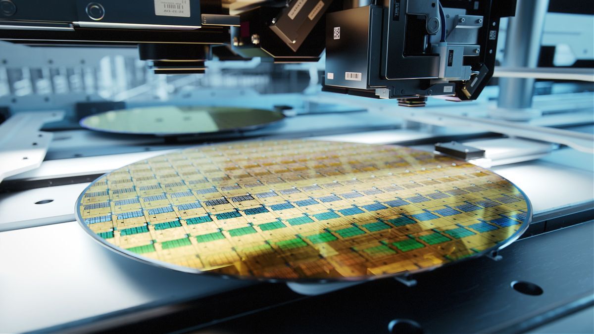
Firm predicts it will cost $28 billion to build a 2nm fab and $30,000 per wafer, a 50 percent increase in chipmaking costs as complexity rises::As wafer fab tools are getting more expensive, so do fabs and, ultimately, chips. A new report claims that


Afaik 2nm is the theoretical limit for current transistor tech so this sort of end-game for this type of tech.
2nm process doesn’t actually mean 2nm though. Hasn’t in over a decade.
The current 3nm process has a 48nm gate pitch and a 24nm metal pitch. The 2nm process will have a 45nm gate pitch and a 20nm metal pitch.
“Nm” is just “generation” today. After 5nm was 3nm, next is 2nm, then 1nm. They’ll change the name after that even though they’re still nowhere near actual nm size.
Where can I read more about this?
Depending on how in-depth you want to delve into this.
Newsletter semianalysis.com
Youtube Asianometry
Wikipedia
Some litography university textbooks. Sadly I don’t know which ones.
Intel already has plans to name the further generations xxA, after Angstroms
Yeah I’m a bit curious what the marketing will be as they have to get more vertical, 3D. Will there be naming to reflect that or will they just follow existing naming, 0.5nm?